About Me
Hey there! I'm Maddie, a final-year Electrical Engineering student at Cal Poly SLO. I'm passionate about control systems, power, and embedded systems.
Through my coursework and personal projects (see below for more!), I’ve gained hands-on industry experience in PCB design, circuit analysis, and hardware debugging where I specialized in Altium, PCB/circuit design, and system integration. I have a strong foundation in the electrical engineering fundamentals, and am looking forward to doing more control systems work in the future.
I’m excited to apply my skills to advanced engineering projects in industry as I prepare to graduate in June 2026.
Outside of engineering, I enjoy skiing, ice hockey, biking, and playing both viola and piano.
Work Experience
Electrical Production Test Intern (June 2024 - September 2024)
San Luis Obispo, CAI had a second internship at Edge Autonomy where I...
- Designed multiple PCBs from initial schematic generation to final production using Altium.
- Used circuit analysis techniques to construct circuit boards used for testing parts in production.
- Integrated ESD protection into PCB designs, developed USB-C power delivery systems, integrating IC controllers for voltage/current regulation onto board.
- Contributed 8 complex Altium footprints/3D models to workspace
- Utilized SolidWorks to create fixtures for PCB testing and assembly.
Electrical Engineer Intern (June 2023 - September 2023)
San Luis Obispo, CAIn my first internship with Edge Autonomy, I...
- Diagnosed and resolved issues with overheating PCBs, including component replacement and validation.
- Initiated the assembly of a ground-based test rig for aircraft system integration.
- Conducted root-cause analysis on faulty batteries and helped implement corrective measures.
- Drafted and executed testing procedures for coaxial cables using a spectrum analyzer.
- Played a key role in resolving non-conformance issues related to air data pods.
- Gained experience with JIRA for tracking project progress and managing tasks within a team.
Projects

Design & Hardware
- SCARA arm (custom 3D-printed parts for longer reach + mini-gripper)
- Arduino Mega 2560 + RAMPS 1.4, A4988 stepper drivers, NEMA-17 motors
- SG90 micro-servo for gripper actuation
- Raspberry Pi 3 Model B and overhead webcam for vision
- USB lighting/speaker for consistent illumination and feedback
- Stockfish Chess Engine for next-best-move algorithms
Software & Vision
- Python on Pi/PC: camera capture, board state, move validation, Stockfish
- Arduino firmware: inverse kinematics + coordinated stepper control
- No embedded board sensors required - pure overhead camera detection
- Supports castling & en passant; prompts user for pawn promotions
Detection Logic
- Square occupancy via RGB pixel variance across board cells
- Piece color classified by average pixel brightness thresholds
- Invalid moves trigger user alerts and re-scan
Practical Notes
- High-contrast board/pieces and even, shadow-free lighting
- Camera calibration (distortion/fisheye) and stable mount
- Manual arm alignment at startup for reference zero
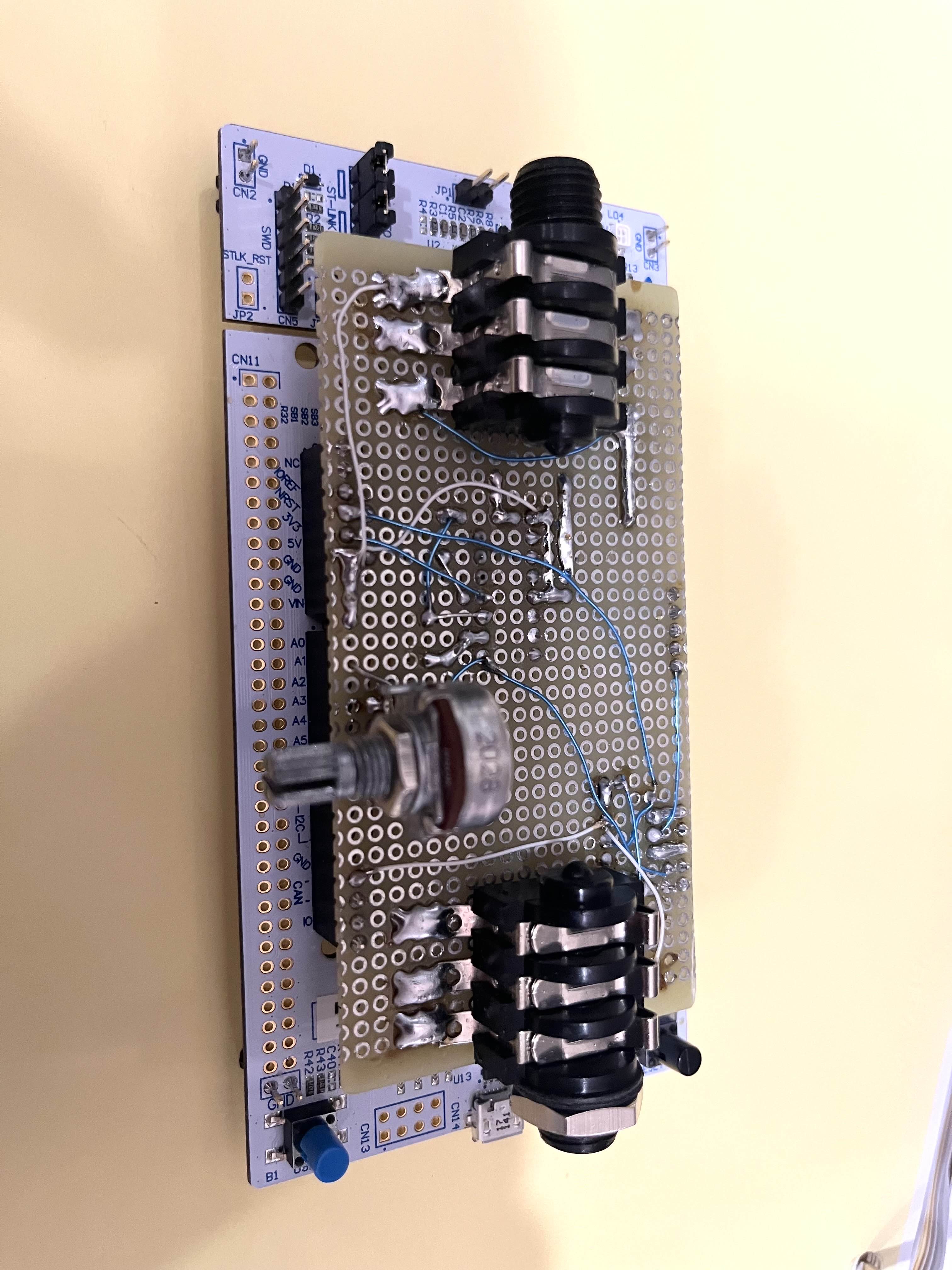
Signal Processing Chain
- Analog guitar input signal conversion via STM32's built-in ADC
- Digital signal storage using circular buffer
- Delayed playback through external DAC
User Controls
- Adjustable delay time via potentiometer
- Feedback control (number of repetitions)
- Dry/wet mix control (balance between original and delayed signals)
- True bypass button for direct signal routing
Key Features
- Real-time parameter adjustment
- Dynamic audio output behavior
- Low latency optimization
- High-fidelity audio performance
- Suitable for both live and studio use
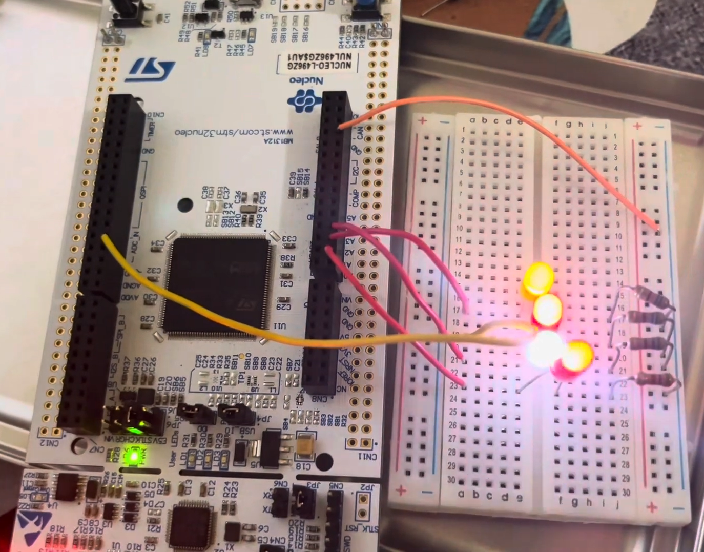
LED Counter Implementation
- 4-bit binary counting from 0 to 15
- Visible delay between count transitions
- Oscilloscope-calibrated delay loop timing
Instruction Timing Analysis
- Execution timing measurements for:
- Various data types
- Different arithmetic operations
- Comprehensive timing results documentation
- Performance analysis and optimization
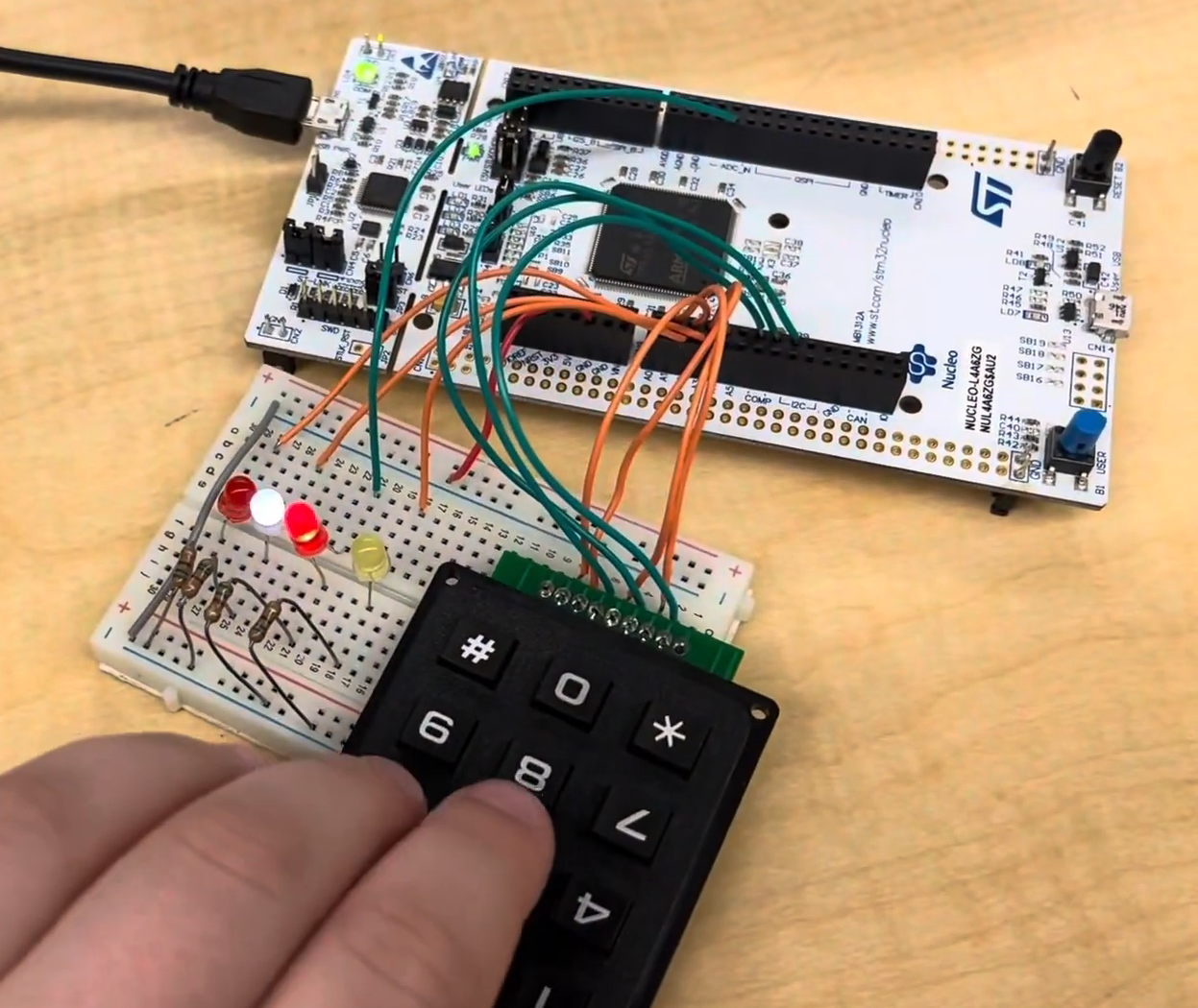
Hardware Integration
- 3x4 matrix keypad connection to GPIO pins
- Four-LED output display system
- Efficient GPIO pin utilization
Software Features
- Polling-based keypress detection
- Software debounce implementation
- 4-bit binary value conversion
- Real-time LED display updates
System Design
- Modular keypad interface architecture
- Robust configuration system
- Efficient keypress detection algorithm
- Reliable input processing pipeline
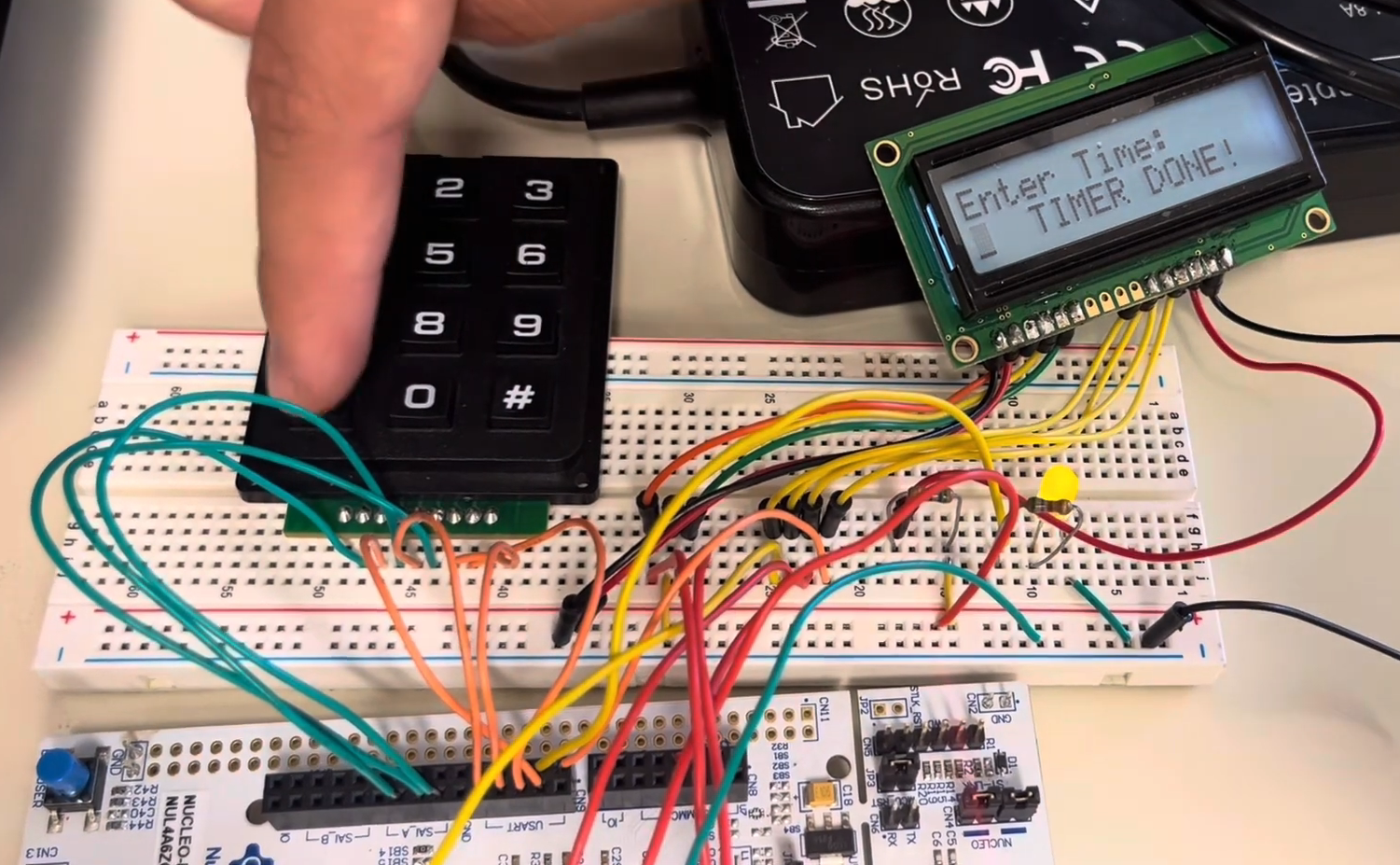
Key Features
- Time input in MM:SS format using keypad (right to left entry)
- Real-time LED feedback with once-per-second flash during countdown
- Special LED "dance" sequence at timer completion
- Comprehensive LCD display interface
System States
- Greeting screen on startup
- Time input mode for setting countdown
- Active countdown state with visual feedback
- Completion state with animation
Technical Highlights
- Optimized delay functions for improved response time
- Precise timing implementation, especially for LCD operations
- Reliable star/reset button functionality with variable press timing
Hardware Setup
- 16x2 LCD display interface
- Onboard button for user input
- LED for visual signaling
- Hardware RNG module utilization
Game Implementation
- 1ms precision timing system
- Randomized delay generation
- Real-time reaction measurement
- Automatic round reset functionality
- LCD-based result display
Technical Architecture
- Interrupt-driven state machine design
- Clean modular code structure
- Responsive timing implementation
- Efficient game loop management
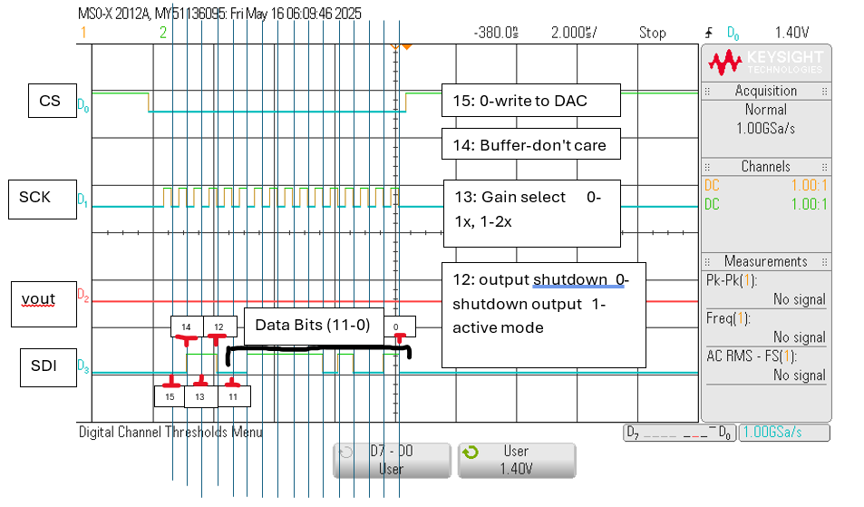
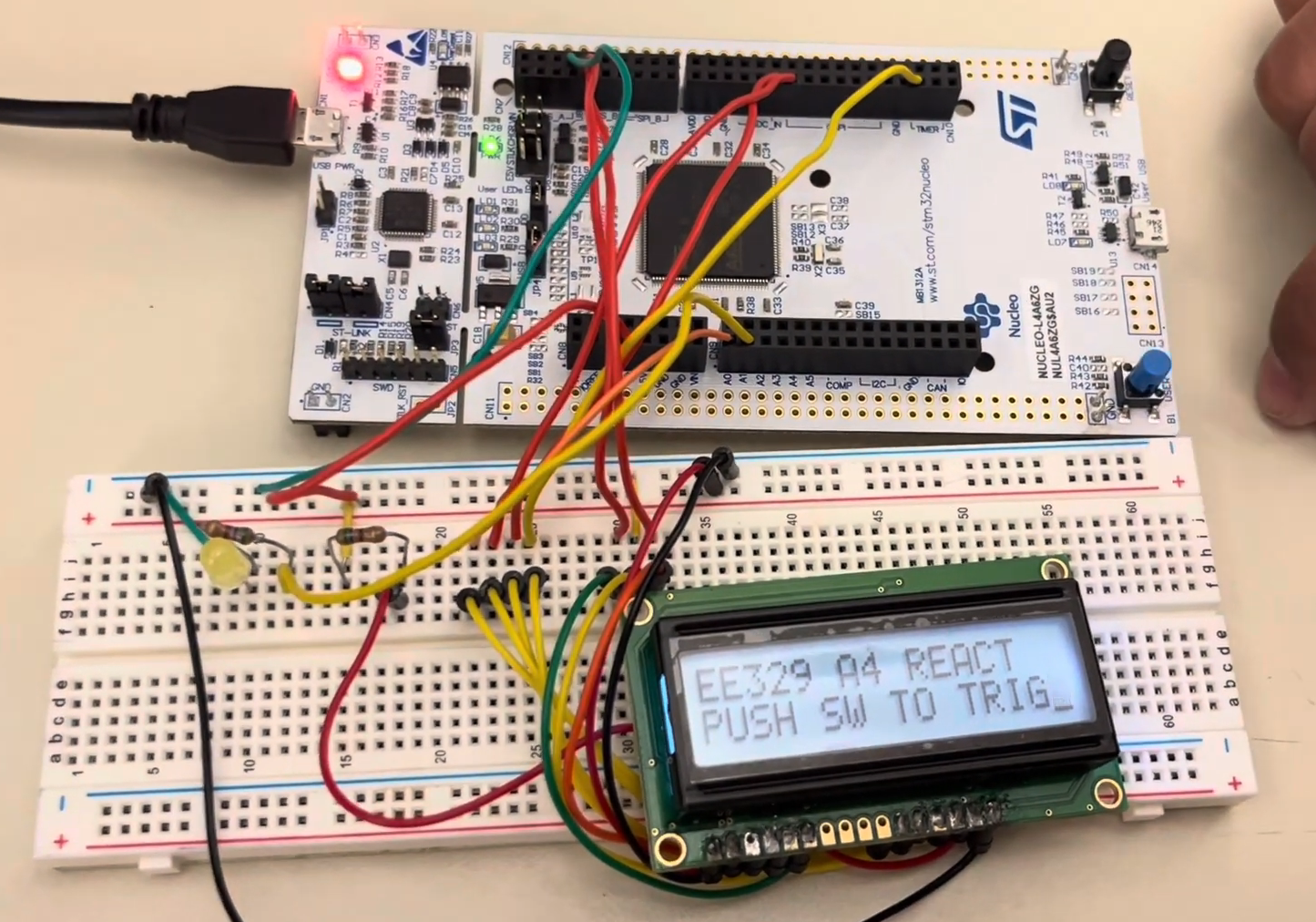
Hardware Integration
- STM32L4 microcontroller as main controller
- MCP4821 DAC for analog output
- 4x3 matrix keypad for user input
- SPI communication interface
Functionality
- Real-time voltage output (0.00V to 3.30V)
- 3-digit voltage value input
- 12-bit DAC word conversion
- Input validation system
- Output voltage capping
- Reset functionality
Verification
- Logic analyzer testing
- Calibration for accuracy
- Comprehensive timing analysis
- Performance requirements validation
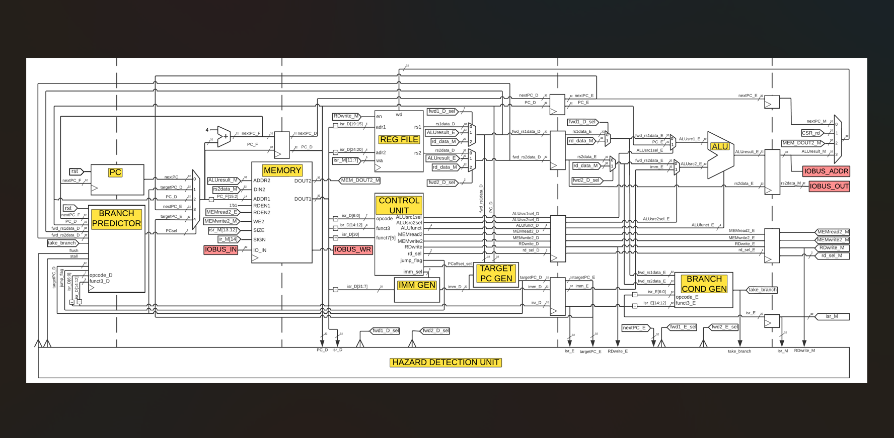
Implementation Details
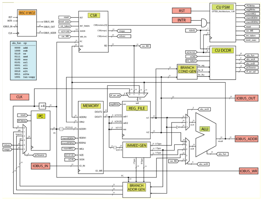
- Hazard Detection and Forwarding:
- Implemented two hazard multiplexers (HazardMuxA and HazardMuxB) in the execute stage
- Enabled operand forwarding to avoid incorrect computation due to RAW hazards
- Hazard unit compares source and destination registers across pipeline stages
- Selects forwarded data from either MEM or WB stage when needed
- Load-Use Hazard Handling:
- Detects when a load instruction is followed by a dependent instruction
- Stalls the PC and decode stage
- Flushes the execute stage to prevent incorrect execution
- Control Hazard Management:
- Implemented static branch-not-taken predictor
- Corrected PC selection logic placement to execute stage
- Added actual_pc_selE computation based on instruction type (branch, JAL, JALR)
- Implemented flush logic to remove misfetched instructions
Verification and Performance
- Waveform analysis confirmed:
- Correct forwarding paths in EX stage
- Proper stall insertion for load-use hazards
- Appropriate flushes and PC redirection for control mispredictions
- Performance comparison with multi-cycle implementation:
- Over 1 million times faster on 50x50 matrix multiplication benchmark
- 93 mW total on-chip power consumption
- Maintained similar resource utilization
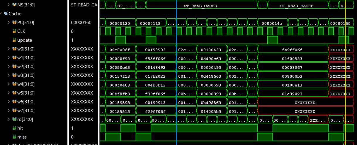
Key Specifications
- Cache Organization: 16 blocks × 8 instructions per block (32-bit words)
- Block Size: 32 bytes total
- Addressing: Direct-mapped with tag + valid bit arrays
- Miss Penalty: One cycle NOP (0x13) + memory fetch time
Implementation Details
- Cache Module:
- Tag tracking and comparison logic
- Critical tag update: tags[index] ⟸ pc_tag for block replacements
- Hit/miss detection with valid bit verification
- Word selection within cache blocks
- State Machine (FSM):
- ST_READ_CACHE: Normal operation with hit handling
- ST_READ_MEM: Miss handling with PC stall
- Automatic state transitions on block fetch completion
- Pipeline Integration:
- Modified IF/ID register and PC update logic
- Combined hazard handling (StallD, StallF) with Cache_stall
- NOP insertion during misses
- Cache-pipeline synchronization
Error Handling
- Cache miss → Immediate pipeline stall
- Invalid cache state → Automatic flush
- Memory fetch failure → Recovery mechanism
- Cache coherency maintenance
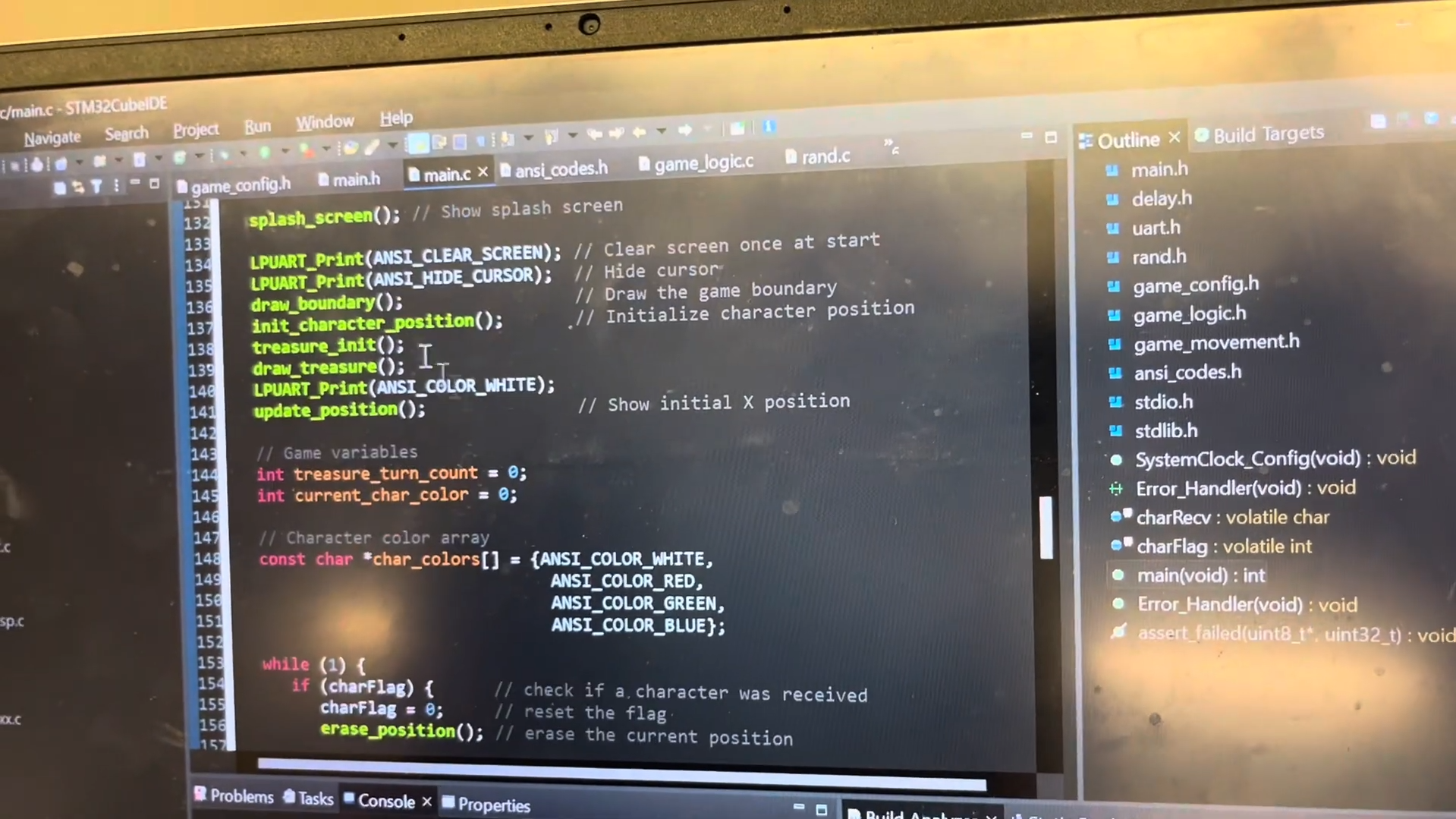
Technical Implementation
- UART communication via GPIO alternate functions
- Terminal interface with character echo capability
- Terminal escape code formatting
- Two-stage development process:
- Initial character echo testing phase
- Full game implementation stage
Game Features
- Interactive player movement controls
- Stick figure character design
- Screen-wrapping border mechanics
- Color-changing mechanics:
- Multi-color player character
- Character turns red for 3 moves after collecting treasure
- Solid border implementation
Development Highlights
- Bug-free implementation
- Practical experience with UART interface
- Terminal formatting with escape codes
- Real-world embedded systems communication
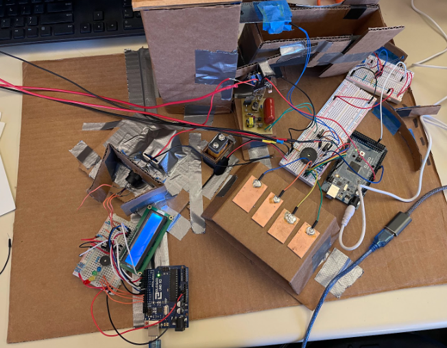
Development Process
- Week-by-week circuit segment implementation
- Iterative design and testing
- Component integration strategy
- Final showcase demonstration
System Features
- Capacitive touch piano input
- Musical passcode system
- Multi-stage activation sequence
- LCD display output
Technical Implementation
- Circuit segment modularity
- Sequential trigger system
- Interactive user interface
- Creative alarm functionality
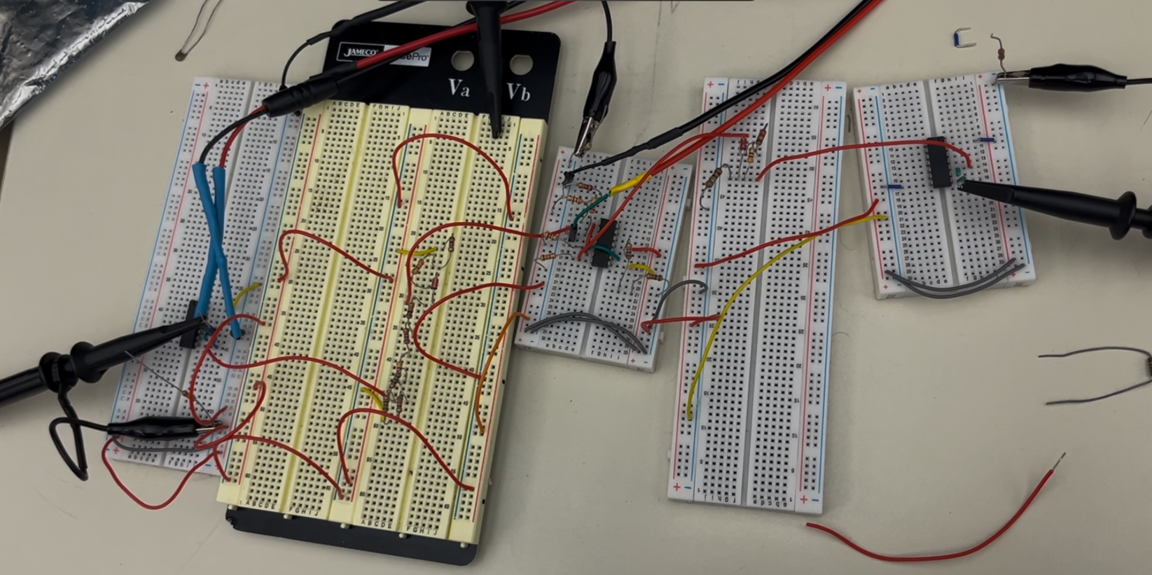
Technologies Explored
- Positive Emitter-Coupled Logic (PECL)
- Transistor-Transistor Logic (TTL)
- Complementary Metal-Oxide-Semiconductor (CMOS)
Implementation Details
- Custom PECL OR-NOR gate construction
- TTL to PECL interface design
- PECL to CMOS integration
- Circuit analysis and optimization
Project Outcomes
- Successful multi-technology integration
- Practical digital logic implementation
- Custom interface validation
- Comprehensive circuit documentation
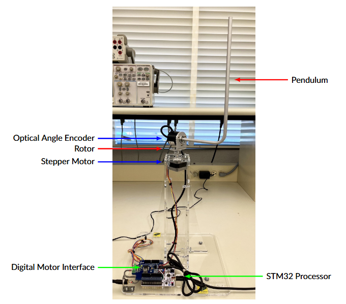
- focused on the behavior of second-order systems by deriving transfer functions and analyzing the effects of poles and zeros on system responses,
- designed a single-input single-output (SISO) controller for the Pendulum angle,
- focused on the application of Root Locus methods to improve transient response behavior,
- designed and implemented a lead compensator to improve transient response, increase stability margins, and enhance overall system performance,
- designed a PID controller that effectively minimizes steady-state error while meeting transient response specifications,
- used two different tuning methods, Manuel and Ziegler-Nichols, to adjust the PID gains (Kp, Ki, and Kd) through simulations and hardware experiments
- utilized frequency response design methods to look at gain and phase margins to help us understand the stability of our system.
Education / Training
Electrical Engineering, B.S. (September 2021 - Present)
San Luis Obispo, CAI am currently pursuing a Bachelor of Science degree in Electrical Engineering at Cal Poly, with a minor in Computer Science. Some of my relevant coursework includes:
- Classical Control Systems (EE 302)
- Vision Based Robots Manipulation & Lab (EE 470/471)
- Microcontroller-Based Systems Design (EE 329)
- Circuits I-III
- Power Systems Analysis I (EE 406)
- Power Electronics & Lab (EE 212/242)
- Energy Conversion Electromagnetics (EE 255)
- Continuous/Discrete Time Signals & Systems (EE 228/328)
- Electromagnetic Fields & Transmission (EE 334/402)
- Computer Hardware Architecture and Design (CSC 333)
- Digital Design and Assembly Programming (CSC 133/233)
- Data Structures (CSC 202)
- Object Oriented Programming (CSC 203
- Semiconductor Device Electronics (EE 306)
- Microprocessor System Design (EE 329)
- Electronic Design & Lab (EE 409/449)
- Analog Electronics & Integrated Circuits & Lab (EE 307/308)